Printed Circuit Board
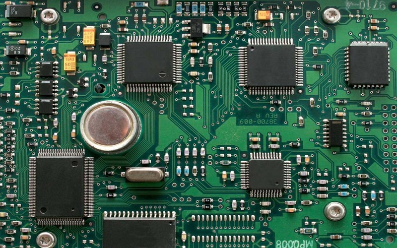
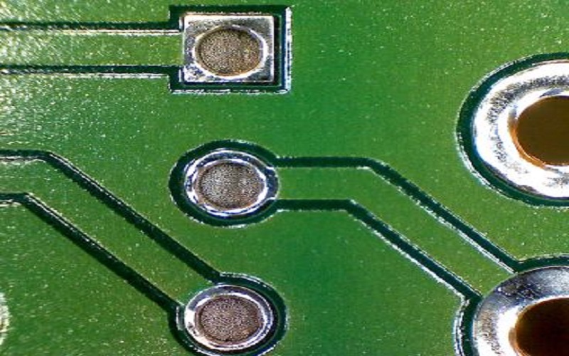
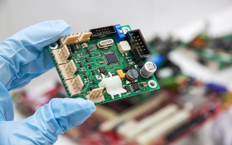
Plating on a Printed Circuit Board (PCB) refers to the electrochemical process by which a metal is deposited onto the surface of the circuit board, and inside the plated through-holes. Copper is the most frequently used metal for PCB plating.
Corrosion Protection
Wear Resistance
Modifying Electrical Conductivity
Improved Adhesion
Friction Modification
Aesthetics
- Lower Contact Resistance
- Protection from Oxidation, Moisture & Contamination
- High Wear Resistance
- Electricity Conductivity

Types of Process
PTH (Plating Through Hole)
Copper Tin Pattern Plating
Electroless Nickel Immersion Gold
Etching
PCB manufacturing process includes etching a copper sheet plated onto a non-conductive substrate and drilling holes through it. These holes will be conductive after the plating process (electroless copper deposition), which will form a thin layer of copper on the walls of the hole.
Typical chemical processes for printed circuit board components:
Alkaline Degreasing
Remove oil, fingerprints, oxides, dust etc. on the surface of the board.
Microetching
Eliminate the oxide layer on the board's surface and roughen it to enhance the adherence between the upcoming copper layer and the substrate's underlying copper.
Preimpregnation
It is mainly done to protect the palladium slot from being polluted from the bath of pre-treatment and extend the shelf life.
Activation
Activation plays a crucial role in determining the quality of the following copper plating.
Desmearing
Eliminate the stannous ion surrounding the palladium particle in the colloid to uncover the palladium core, allowing it to effectively catalyze the creation of the plated-through hole.
Electroless plating
A layer of chemical copper will be deposited on the surface of the board or the wall of the hole.
We specialise in designing and manufacturing NADCAP-approved surface finishing plants for a range of chemical processes:
Anodizing
Hard Chrome Plating
Zinc/Nickel Plating
Cadmium Plating
Electroless Nickel Plating
Passivation
Types of Plants
Rack Plant
Types of Plants
Barrel Plant
Types of Plants
Rack-Barrel Combination
